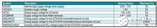
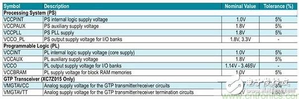
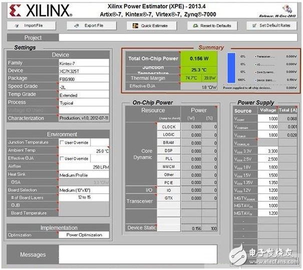
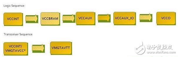
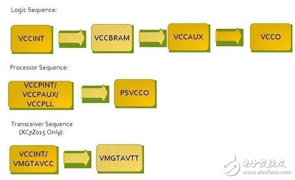
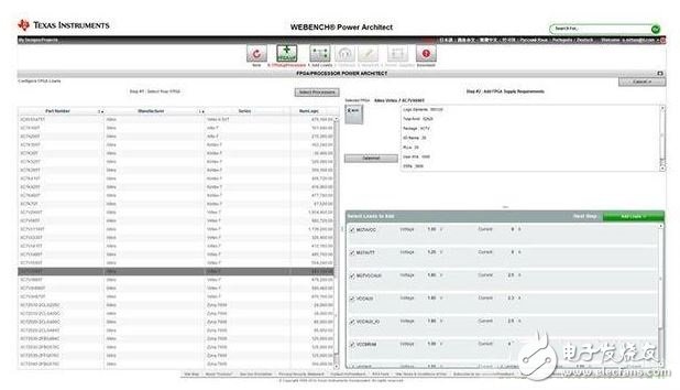
Field Programmable Gate Arrays (FPGAs) can include thousands of typical, programmable logic cells, with a matrix of lines and programmable switches interconnected with separate logic cells. Typical designs include simple logic that specifies each cell. Functionally and selectively turn off the switches in the interconnect matrix. FPGAs are primarily used in prototype IC systems. When the design is complete, designers can convert logic to hard-wire ICs that operate at higher speeds. In order to function properly, FPGAs must employ appropriate power management techniques. Designing a power system for a field programmable gate array (FPGA) is not an easy task. FPGAs are highly configurable semiconductor devices that are used in a wide range of applications and end markets. Common examples include communications, automotive, industrial, medical, video, and defense applications. Due to their high configurability, different components can be placed around them to form the final system design. While there may be countless applications and systems, one common feature of all designs is that they all require power. It is usually necessary to have several voltage rails to power the FPGA. Depending on the application, the main input power supply can be backplane power, isolated power, non-isolated power, or even battery powered. These main inputs typically generate an intermediate DC voltage to power the FPGA's main rail. These intermediate voltages are typically DC voltages of 5V or 12V. Some typical voltage rails, voltages, and tolerance values ​​for FPGAs are listed in Tables 1 and 2. Table 2: Power requirements for Virtex 7FPGA. Table 2: Power requirements for the Zynq 7000 Series System-on-Chip (SoC). Determining the appropriate current level for each voltage rail is a tricky task because the current can range from a few hundred milliamps to 60A or even higher. If you plan ahead, the situation will be completely different. Planning in advance can avoid over-designing the power rail, avoiding spending too much, or avoiding inadequate design, which leads to the need to overturn and other errors. FPGA vendors provide accurate tools that estimate the worst-case power consumption based on how customers use the FPGA. The Xilinx Power Estimator (XPE) shown in Figure 1 covers several Xilinx FPGA families. With this tool, the customer can select the part being used and enter the clock and configuration information to determine the power requirements and select the appropriate device based on the estimate. Figure 1: Power Estimator Tool. Design considerations When choosing a power supply that meets the needs of an FPGA application, many factors must be taken into account. Cost, size, and efficiency are always factors to be aware of during power supply design. However, some power rails will have different requirements in FPGA applications. Kernel power rails typically require tighter accuracy over the line, load, and temperature range. Some power rails, such as transceivers, are more sensitive to noise and need to keep their output below a specific noise threshold. It should also be noted that some power rails with common mode voltages can be combined and isolated with a ferrite bead for filtering or as a load switch. When designing to meet tolerance requirements, all fixed and dynamic operating conditions need to be taken into account. First, choose a regulator with less than 1% reference accuracy, which leaves the customer with the largest design margin to handle dynamic operating conditions such as load transients. Care should also be taken when designing high-speed transceiver power rails because noise on these sensitive power rails can degrade performance and increase jitter. Low dropout regulators (LDOs) are ideal for these power rails. However, when higher currents are required, a switching power supply can be used as long as the typical value of the output ripple remains below 10 mVpk-pk over the frequency range of 10 kHz to 80 MHz. The dedicated FPGA data sheet will contain detailed technical specifications related to transceiver requirements. Power sequencing is another important aspect of FPGA power supply design. Since there are several power rails that power the FPGA, the recommended power sequence below draws the minimum current at startup, which in turn prevents damage to the device. Figure 2 shows a recommended power-up sequence for logic circuits and transceiver power rails on Virtex 7 Series FPGAs. The processor sequencing for the Zynq 7000 Series SoC is shown in Figure 2. Figure 2: Recommended power-up sequence for Virtex 7 FPGAs. *VCCINT and VMGTAVCC can be powered up at the same time, as long as they are started before VMGTAVTT, their power-up sequence can be interchanged. Figure 3: Recommended power-up sequence for the Zynq 7000 Series SoC. For Xilinx 7/Zynq 7000 series devices, these rails must have a monotonic rise and must be powered from 0.2ms to 50ms, while for the Xilinx Ultrascale FPGA family, this period is 0.2ms. It is between 40ms. It is recommended that the power-off sequence be reversed from the power-up sequence. Power solution Once the appropriate current level has been estimated and all design considerations are known, the power supply designer can begin device selection. There are several options to choose from, such as low dropout regulators (LDOs), switch mode power supplies (SMPS), and integrated modules, all with different advantages and disadvantages. For example, due to its simplicity and low output noise, LDOs are ideal for some lower current FPGA power rails. The disadvantage of LDOs is that they are not efficient and will dissipate a large amount of heat through the pass transistors at higher currents. They are generally suitable for applications with lower power and those that require low noise. When the required current value is greater than 2 amps and efficiency is more important, the designer can choose a switch mode power supply (SMPS). These devices can achieve efficiencies in more than 90% in a single phase configuration and provide up to 30A. They are more designed to work with LDOs and are less efficient at lighter loads, but they are more flexible and more efficient at higher current levels. Power modules, such as the LMZ31506 simple switcher, can integrate a DC/DC converter, power metal oxide field-effect transistor (MOSFET), a shielded inductor, and passive components in a thin quad flat no-lead (QFN) inside the package. Design time is reduced because all components are already integrated into one package and only a minimum of external components are required. Webench FPGA Architecture Design Tool The Webench FPGA Architecture Design Tool (Figure 4) is a very useful tool to help power supply designers build several FPGA power rails in minutes. This tool contains detailed power requirements for some of the recently released FPGAs. In this tool, you simply select the FPGA you are using and adjust the current to the required level, and the tool will form a comprehensive design report. Figure 4: Webench FPGA Architecture Design Tool. Array Speakers,Line Array Speaker,Linear Array Loudspeaker,Linear Array Loudspeaker System The ASI Audio Technology Co., Ltd , https://www.asi-sound.com