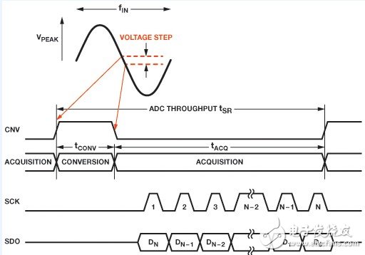
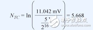
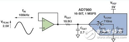
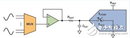
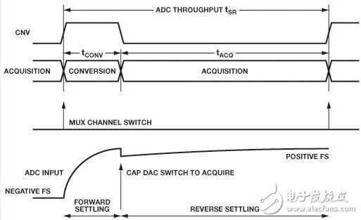
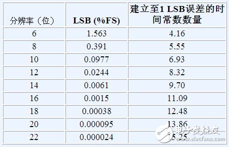
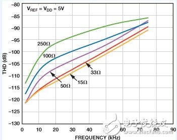
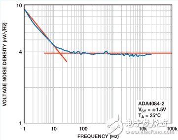
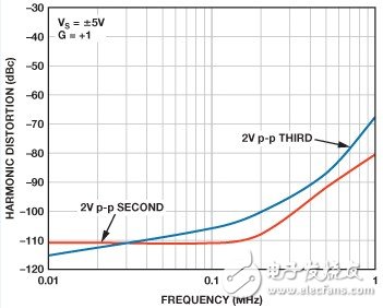
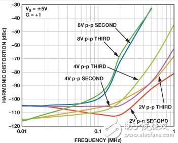
The front-end device of the SAR analog-to-digital converter consists of two parts: a driver amplifier and an RC filter. The amplifier regulates the input signal while acting as a low impedance buffer between the source and the ADC input. The RC filter limits the out-of-band noise reaching the ADC input, helping to attenuate the kickback effects of the switched capacitors at the ADC input. Choosing the right amplifier and RC filter for the SAR ADC can be difficult, especially when the application is different from the general purpose of the ADC data sheet. Based on various application factors that affect amplifier and RC selection, we provide design guidelines for the best solution. Key considerations include input frequency, throughput rate, and input multiplexing. To choose the appropriate RC filter, you must calculate the RC bandwidth for a single channel or multiplexed application and then select the values ​​for R and C. Figure 1 shows a typical amplifier, single-pole RC filter, and ADC.ADC input to form a switched-capacitor load for the driver circuit. Its 10 MHz input bandwidth means low noise is guaranteed over a wide bandwidth to achieve a good signal-to-noise ratio (SNR). The RC network limits the bandwidth of the input signal and reduces the amount of noise that the amplifier and upstream circuitry feed into the ADC. However, too much bandwidth limitation can increase setup time and distort the input signal. Figure 1. Typical Amplifier, RC Filter, and ADC The minimum RC value required to establish the ADC input and limit the noise by optimizing the bandwidth can be calculated by assuming that the step input is established exponentially. To calculate the step size, you need to know the input signal frequency, amplitude, and ADC conversion time. The conversion time tCONV (Fig. 2) refers to the time required for the capacitive DAC to disconnect from the input and perform a bit determination to generate a digital code. At the end of the conversion time, the capacitive DAC with the same charge before switching is switched back to the input. This step change represents the amount of change in the input signal during this time. The time required for this step to build is called the "reverse setup time". Figure 2. Typical Timing Diagram for an N-Bit ADC At a given input frequency, the maximum undistorted rate of change of a sine wave signal can be calculated by: If the conversion rate of the ADC greatly exceeds the maximum input frequency, the maximum amount of change in the input voltage during the conversion is: This is the maximum voltage step that occurs when the capacitive DAC switches back to acquisition mode. Then, a parallel combination of the DAC capacitor and the external capacitor attenuates this step. Therefore, the external capacitor must be relatively large, reaching a few nF. This analysis assumes that the effect of the on-resistance of the input switch is negligible. The step size that needs to be established now is: Next, calculate the time constant of the ADC input to 1â„2LSB during the ADC acquisition phase. Assuming the step input is established exponentially, the required RC time constant Ï„ is: Where tACQ is the acquisition time and NTC is the number of time constants required to establish. The number of time constants required can be obtained by calculating the step size VSTEP and the natural logarithm of the ratio of the establishment error (in this case 1â„2LSB): therefore, Substituting the above formula into the previous formula gives: Equivalent RC bandwidth = Example: Using the RC bandwidth calculation formula, select the 16-bit ADC AD7980 (shown in Figure 3) with a conversion time of 710 ns, a throughput rate of 1 MSPS, and a 5 V reference. The maximum target input frequency is 100 kHz. The maximum step at which this frequency is calculated: Then, the charge of the external capacitor will attenuate this step. Using a 27 pF DAC capacitor and assuming an external capacitance of 2.7 nF, the attenuation factor is approximately 101. Substituting these values ​​into the VSTEP calculation formula: Next, calculate the number of time constants established to 1â„2 LSB (16-bit, 5 V reference): The acquisition time is: Calculate Ï„: Therefore, the bandwidth is 3.11 MHz and the REXT is 18.9 Ω. Figure 3. RC filter with 16-bit 1 MSPS ADC AD7980 This relationship between minimum bandwidth, throughput rate, and input frequency indicates that the higher the input frequency, the higher the RC bandwidth is required. Similarly, the higher the throughput rate, the shorter the acquisition time, which increases the RC bandwidth. Acquisition time has the greatest impact on the required bandwidth; if the acquisition time is doubled (reducing the throughput rate), the required bandwidth will be halved. This simplified analysis does not include the second-order charge recoil effect, which becomes the main influencing factor at low frequencies. When the input frequency is very low (<10 kHz, including DC), a voltage step of approximately 100 mV is always established on the capacitive DAC. This value should be used as the minimum voltage step for the above analysis. Multiplexed input signals are rarely continuous and are typically composed of large steps resulting from different channel switching. In the worst case, one channel is at negative full scale and the next channel is at full full scale (see Figure 4). In this case, when the multiplexer switches channels, the step size will be the full scale of the ADC, which is 5 V for the above example. Figure 4. Multiplexing settings When using a multiplexed input in the above example, the filter bandwidth required for the linear response will increase to 3.93 MHz (the step size is 5 V instead of 1.115 V for a single channel). The assumptions are as follows: The multiplexer switches shortly after the start of the conversion (Figure 5), and the amplifier and RC forward settling time is sufficient to stabilize the input capacitance before the acquisition begins. Figure 5. Multiplexing timing For the calculated RC bandwidth, it can be checked using Table 1. As can be seen from the table, to establish the full-scale step to 16 bits, 11 time constants are required (see Table 1). For the calculated RC, the forward settling time of the filter is 11 × 40.49 ns = 445 ns, which is much less than the conversion time of 710 ns. The forward setup does not need to occur all during the conversion period (before the capacitive DAC switches to the input), However, the sum of the forward and reverse settling times should not exceed the required throughput rate. For low frequency inputs, the rate of change of the signal is much lower, so the positive set up is not very important. Table 1. Number of time constants required to establish resolution to N bits After calculating the approximate bandwidth of the filter, you can select the values ​​of REXT and CEXT, respectively. The above calculation assumes CEXT = 2.7 nF, which is typical for the application circuit shown in the data sheet. If a larger capacitor is selected, the attenuation of the kickback will be greater when the capacitive DAC is switched back to the input. However, the larger the capacitance, the more likely the driver amplifier becomes unstable, especially when the REXT value is small for a given bandwidth. If the REXT value is too small, the amplifier's phase margin will decrease, which may cause the amplifier output to ring or become unstable. For loads with a small series REXT, a low output impedance amplifier should be used to drive. Stability analysis can be performed using the RC combination and the Bode plot of the amplifier to verify that the phase margin is sufficient. It is best to choose a capacitor value of 1 nF to 3 nF and a reasonable resistor value to keep the driver amplifier stable. Also be sure to use a low voltage coefficient capacitor, such as the NP0 type, to maintain low distortion. The value of REXT must be such that the distortion level remains within the required range. Figure 6 shows the effect of drive circuit resistance on distortion as a function of the AD7690 input frequency. Distortion increases as the input frequency and source resistance increase. The cause of this distortion is mainly the nonlinear nature of the impedance provided by the capacitive DAC. Figure 6. Effect of source resistance on THD versus input frequency A low input frequency (<10 kHz) can support large series resistance values. Distortion is also related to the input signal amplitude; for the same distortion level, the lower amplitude can support higher resistance values. Calculate REXT in the above example: Ï„ = 51.16 ns, assuming CEXT is 2.7 nF, and the resistance value is 18.9 Ω. These values ​​are close to the common values ​​given in the Applications section of the ADI data sheet. The nominal RC value calculated here is a useful guide, but not the final solution. Choosing the right balance between REXT and CEXT requires an understanding of the input frequency range, how much capacitance the amplifier can drive, and the acceptable level of distortion. In order to optimize the RC value, it must be tested with actual hardware to achieve the best performance. In the previous section, we calculated the RC bandwidth for the ADC input based on the input signal and ADC throughput rate. This information must then be used to select the appropriate ADC driver amplifier. Need to consider the following aspects: ·Amplifier size signal bandwidth ·Settling time ·Amplifier noise characteristics and effects on system noise ·distortion · Distortion for power rail margin requirements This data sheet usually gives the small signal bandwidth of the amplifier. However, depending on the type of input signal, large signal bandwidths may be more important, especially for high input frequencies (>100 kHz) or for multiplexed applications (because voltage swings are more Large), and the positive establishment of the input signal is more critical. For example, the ADA4841-1 has a small signal bandwidth of 80 MHz (20 mV pp signal), but a large signal bandwidth of only 3 MHz (2 V pp signal). The above example uses the AD7980 with a calculated RC bandwidth of 3.11 MHz. For lower input frequencies, the ADA4841-1 is a good choice because its 80 MHz small signal bandwidth is more than sufficient for reverse setup, but is multiplexed There are difficulties in the application, because for large signal swings, the RC bandwidth requirement is increased to 3.93 MHz. In this case, the more suitable amplifier is the ADA4897-1, which has a large signal bandwidth of 30 MHz. In general, the amplifier's small/large signal bandwidth should be at least two or three times larger than the RC bandwidth, depending on whether it is built in reverse or forward. If the amplifier stage is required to provide voltage gain (which reduces the available bandwidth), this principle is more applicable and may even require a wider bandwidth amplifier. Another way to look at the forward build requirements is to look at the settling time characteristics of the amplifier, which usually refers to the time required to establish a certain percentage of the nominal step size. For 16-bit to 18-bit performance, it is usually required to build to 0.001%, but most amplifiers only specify 0.1% or 0.01% settling time for different step sizes. Therefore, in order to determine whether the build feature supports the ADC throughput rate, these values ​​need to be compromised. The ADA4841-1 gives a 0.01% settling time of 1 μs for an 8 V step. In a multiplexed application that drives the 1 MSPS (1 μs period) AD7980, it will not be able to set the full-scale step input in time. However, if the throughput rate is reduced, for example 500 kSPS may be feasible. The RC bandwidth is important to determine the maximum allowable noise level of the amplifier. Amplifier noise is typically specified by low frequency 1/f noise (0.1 Hz to 10 Hz) and broadband noise spectral density at high frequencies (flat portion of the noise curve shown in Figure 7). Figure 7. ADA4084-2 voltage noise vs. frequency The total noise that is converted to the input of the ADC can be calculated as follows. First, calculate the noise of the amplifier's wideband spectral density over the RC bandwidth. Where en = noise spectral density (V/Hz), N = amplifier circuit noise gain, BWRC = R bandwidth (Hz) Then, the low frequency 1/f noise is usually calculated by the following equation; it is usually specified as the peak-to-peak value and needs to be converted to the root mean square value. Where = 1/f peak-to-peak noise voltage, N = amplifier circuit noise gain. The total noise is the sum of the squares of the above two noises: To minimize the effects of driver noise on the overall SNR, this total noise should be around 1/10 of the ADC noise. Higher noise may also be allowed depending on the SNR requirements of the target system. For example, if the ADC has an SNR of 91 dB and VREF = 5 V, the total noise should be less than or equal to This value makes it easy to calculate the maximum allowable value of 1/f noise and broadband noise spectral density. Suppose the amplifier to be used has negligible 1/f noise, operates at unity gain, and uses a filter with an RC bandwidth of the above example (3.11 MHz), then Therefore, the amplifier's wideband noise spectral density must be less than or equal to 2.26 nV/√Hz. The wideband noise spectral density of the ADA4841-1 is 2.1 nV/√Hz, which meets this requirement. Another important feature that amplifiers need to consider is the distortion at a particular input frequency. Typically, for best performance, a 16-bit ADC requires approximately 100 dB of total harmonic distortion (THD) and an 18-bit ADC requires approximately 110 dB. Figure 8 shows typical distortion and frequency of the ADA4841-1 for a 2 V pp input signal. Diagram of the relationship. Figure 8. Distortion vs. Frequency for the ADA4841-1 The figure shows not the total harmonic distortion, but the most important secondary and third harmonic components. The ADA4841-1's very low noise and excellent distortion characteristics are sufficient to drive an 18-bit ADC to approximately 30 kHz. When the input frequency is close to 100 kHz or higher, the distortion performance begins to degrade. To achieve low distortion at high frequencies, you need to use an amplifier that consumes more power and has a wider bandwidth. Larger signals also degrade performance. For ADC inputs from 0 V to 5 V, the distortion performance signal range will increase to 5 V pp. As can be seen from the distortion plot shown in Figure 8, this will produce different performance, so the amplifier may need to be tested to ensure it meets Claim. Figure 9 compares the distortion performance of multiple output voltage levels. Figure 9. Distortion vs. Frequency at Different Output Voltage Levels The margin, the difference between the amplifier's maximum actual input/output swing and the positive and negative rails, may also affect the THD. The amplifier may have rail-to-rail inputs and/or outputs, or require a margin of up to 1 V or more. Even for rail-to-rail input/output, if the operating signal level is close to the amplifier's supply rail, it will be difficult to achieve good distortion performance. Therefore, it is best to choose the power supply level that keeps the maximum input/output signal away from the rail. Considering an ADC with a 0 V to 5 V input range, driven by an ADA4841-1 amplifier, the ADC range needs to be maximized. The amplifier has a rail-to-rail output with a 1 V margin requirement for the input. If used as a unity-gain amplifier, at least 1 V of input margin is required, and the positive supply must be at least 6 V. The output is rail-to-rail, but can only be driven to approximately 25 mV of ground or positive supply rails, thus A negative supply rail is required to drive to ground all the time. In order to leave a certain margin for the distortion performance, the negative supply rail can be -1 V. Negative power can be eliminated if the ADC input range is allowed to be reduced, thereby losing some SNR. For example, if the input range of the ADC drops to 0.5 V to 5 V, this 10% loss will result in a SNR reduction of approximately 1 dB. However, this will ground the negative supply rail, eliminating the circuitry used to generate the negative supply and reducing the power. Consumption and cost. Therefore, when selecting an amplifier, it is important to consider the input and output signal range requirements in order to determine the required supply voltage. In this example, an amplifier rated for 5 V does not meet the requirements; however, the ADA4841-1 is rated at 12 V, so using a higher supply voltage will provide excellent performance and provide adequate power headroom. Car Connector,Smt Patch Car Connector,Waterproof Patch Car Connector,Automotive Car Connector Shenzhen Jinyicheng Electronci Technology Co.,Ltd. , https://www.jycconnector.com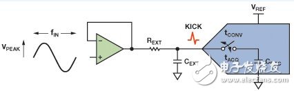
Three main aspects to consider when selecting a precision SAR ADC
Foreword