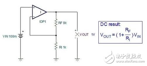
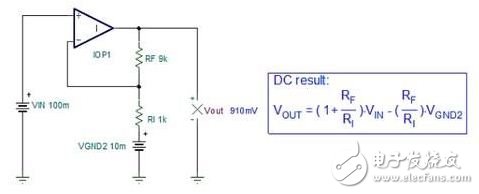
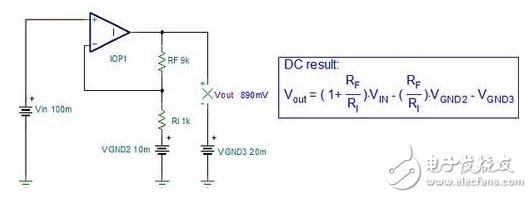
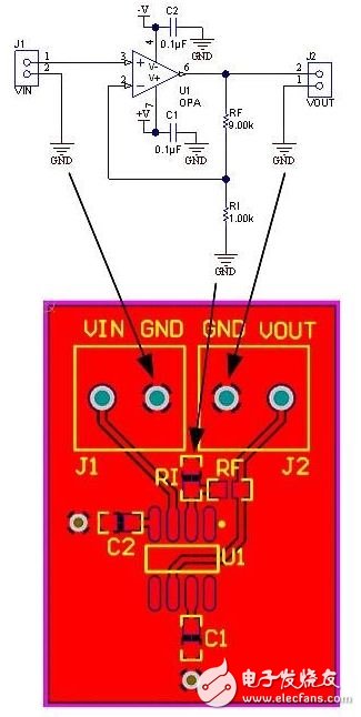
When drawing a schematic, people always take some care of the system ground loop (or GND) symbol. The GND symbol extends throughout the schematic and the schematic assumes that different GNDs will be at the same potential on the printed circuit board (PCB). In fact, the current through the GND impedance creates a Voltage difference between the GND connections on the PCB. Single-ended dc circuits are especially sensitive to these GND dropouts because the expected single-ended circuit can be turned into a differential circuit, resulting in output errors. We use the standard non-inverting amplifier circuit shown below as an example. Applies to our familiar circuit gain 1+RF/RI when the input supply VIN and the input resistor RI have the same GND potential. Therefore, multiplying the 100mV input signal by 10V/V is equal to the 1V output. In the circuit shown below, a voltage source VGND2 is inserted between the input power supply GND and the RI GND connection. Result = Modified Transfer Function + VGND2 Voltage & TImes; - RF/RI Inverting Circuit Gain. A 10mV GND potential difference reduces the required 1V output by 90mV to 0.91V. This is equivalent to a relative error of 9% compared to the required 1V output. In the circuit shown below, the transfer function is further affected when the output voltage is referenced to the third GND potential, VGND3. The VGND3 voltage is subtracted directly from the previous output transfer function. So the 20mV VGND3 voltage reduces the output voltage to 890mV compared to the required 1V output, which is equivalent to 11% error. Using the appropriate PCB layout techniques, the circuit input supply, input resistors, and GND of the output voltage are at the same potential, which reduces the problems in the above two examples. The best solution is to use the common "star" GND method to make important GND connections physically close together. This will reduce the PCB impedance generated between the GND connections, which in turn reduces any voltage potential differences between them. In the example schematic and layout shown below, the input supply, the output voltage, and the GND connection to the input resistor are all on the top of the PCB. This prevents single-ended circuits from becoming differential circuits! In summary, the next time there is any dc circuit performance problem, check that the voltage potentials of all important GND connections are equal. At present, Lithium Polymer Battery is advanced rechargeable secondary battery . With cathode materia l- LiCoO2, LiMn2O ,Li(NiCoMn)O2, and anode material - C, Lithium Polymer battery has many merits: Good safety performance, high energy density, excellent charge retention, long cycle life, low self-discharge rate, low resistance, no memory effect and non-pollution.Lithium Polymer Battery is main applied for various customer electronic products, such as phone, smart security products, POS machine, GPS tracker and so on. Lithium Polymer Battery Lithium Polymer Battery,Mobile Battery,Rechargeable Lithium Polymer Batteries,Small Lithium Polymer Battery Ji'an Powercom New Energy Co., Ltd. , https://www.expowercome.com