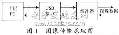
introduction Traditional image transmission is generally implemented by various interfaces provided by the PC motherboard, such as PCI interface, EPP interface, IEEE 1394 interface, etc. The maximum rate of the PCI interface can reach 132 Mb / s, but its installation is cumbersome, expensive, and has poor scalability. It cannot be specifically electromagnetically shielded, and its speed is not ideal in high-speed transmission. The EPP interface does not require other cards in the PC, and can be connected without limit. The equipment is easy to install and use, but the maximum rate is only 2 Mb / s, and the speed is relatively slow. It is mainly used for low-end performance requirements. The IEEE 1394 interface allows connection of a variety of high-performance devices, interconnecting its high-performance bus, with a transmission rate of up to 400 Mb / s, of which IEEE 1394 b can reach 3.2 Gb / s, mainly used in high-speed video or without peripheral When connected to a PC, the peripheral circuit is complicated and expensive. The Universal Serial Bus (USB) corresponding to the above interface has a data rate significantly higher than that of the general serial port. It can support four data transmission methods: control, interrupt, synchronization, block transmission, and hot plug. Plug and play, and has the advantages of less system resources, low power consumption, and reliable data transmission. USB bus technology is to use a single bus technology to meet the needs of a variety of applications. USB 1.1 protocol supports two transmission speeds, namely low speed 1.5 Mb / s and full speed 12 Mb / s. The USB 2.0 protocol released in 2000 is backward compatible with the USB 1.1 protocol. The maximum data transfer rate can reach 480 Mb / s, which can continuously expand the range of USB applications. The system is based on USB 2.0 bus technology and combines the Slave FIFO block transfer interface mode of the CY7C68013A chip with FPGA technology to achieve high-speed image data transmission between the computer and peripheral devices. 1 System design 1.1 Hardware and peripheral control design The main chip to realize the USB interface unit is CY7C68013A in the EZ-USB FX2LP series of CYPRESS (compared to the previous FX2 series CY7C68013 with lower power consumption, smaller current, high cost performance, etc.), responsible for completing the hardware system and PC Image transmission. It has three interface modes with the outside: port mode, programmable interface GPIF and Slave FIFO. Slave FIFO is a slave working mode. In devices with external data processing logic, USB data is transmitted between the host and external logic devices. Usually, the CPU of FX2LP is not required to participate, but it is transmitted through the FX2LP internal endpoint FIFO. The external controller can choose to read and write to the FIFO of multiple endpoints. The working mode of Slave FIFO of FX2LP can be set to synchronous or asynchronous; the working clock can be generated internally or input externally. The system is based on the transmission of high-speed images, which requires an external controller to directly control the FIFO, so the slave, that is, Slave FIFO mode is used. The principle block diagram of high-speed image transmission is shown in Figure 1. First, the image can be sent or received by the upper application software of the computer, and then connected to the cache through the USB interface chip. The USB interface in Figure 1 uses the Slave FIFO of the CY7C68013A chip. The interface mode enables high-speed communication between the upper-layer PC and the buffer, and FPGA is used to control the high-speed transmission of USB. As shown in Figure 2, the main function signals of CY7C68013A and the handshake signal with FPGA such as: IFCLK is a clock signal, which can be selected from external input or internal output; FIFOADR [1: 0] pin selects 4 FIFO (2, One of 4, 6 or 8) is connected to the USB data bus FD. Define the upstream data transmission in this system as FIFOADR [1: 0] = 10, which is the EP6 port; the downstream data transmission as FIFOADR [1: 0] = 01, which is the EP2 port. FLAGB, FLAGC is the flag signal of the selected FIFO, FLAGB represents the FIFO is full; FLAGC represents the FIFO is empty; the default low level is effective. The FPGA can determine whether to perform a read or write operation by continuously querying these two flag signals. SLOE is a read / write enable signal; SLWR and SLRD are read and write control signals, respectively, in synchronous and asynchronous modes, the control signals are different; FD [15: 0] is a 16-bit bidirectional data bus. PA0 and PA1 are output signals, which are used as control signals for the working state of the hardware system.
5MM RGB LED is the most popular LED in Through-hole RGB LED.
Same as the 3mm RGB LED, 5mm RGB LED also have three chips in, four pins, common cathode or common anode and those chips can be placed arbitrarily.
The shape of the lens can be 5mm round RGB LED, 5mm Straw hat RGB LED, 5mm pointed top RGB LED and 5mm round LED without flange RGB LED.
For the 5mm RGB LED, the lens can be water clear or diffused. The former has a strong spotlight, and the later lens will make people feels soft.
5mm RGB LED 5mm RGB LED, RGB Dip LED Diode 5mm, 5mm Digital RGB LED, Red Through Hole RGB LED 5mm Shenzhen Best LED Opto-electronic Co.,Ltd , https://www.bestsmd.com