Digital power amplifier circuit and anti-interference design based on TDA8902J 1. PCB layout and wiring principles PCB provides electrical connections between components of the power amplifier circuit. To achieve the best performance of the power amplifier circuit, the layout of the components and the layout of the printed wires are the key. (2) The components should be arranged in the order of output filter, H-bridge circuit, comparator, oscillation generator, and voltage amplifier. If the various levels are arranged in a cross, it is easy to affect each other and cause self-excitation or absorption. 2. Anti-interference design measures The PCB anti-interference design has different requirements for different circuits. The following discusses the PCB anti-interference design measures of the power amplifier from three aspects. 3. Electromagnetic compatibility (EMC) design The digital power amplifier based on TDA8902J has high power, low heat loss, good sound quality, and small size. After electromagnetic compatibility design of its PCB, the sound quality is better, the signal-to-noise ratio is higher, and the anti-interference ability is also significantly enhanced. It can be applied to many Audio equipment, such as sound cards, active speakers, car audio, etc., has broad prospects. 4. Conclusion The digital power amplifier based on TDA8902J has high power, small heat loss, good sound quality and small size. After the electromagnetic compatibility design of its PCB, the sound quality is better, the signal-to-noise ratio is higher, and the anti-interference ability is also significantly enhanced. It is used in many audio equipment, such as sound card, active speaker, car audio, etc., and has broad prospects.
Solar road light is a crystalline silicon solar battery power supply, valve control type sealed and maintenance-free battery, gel battery) to store electrical energy, super bright LED as light source, lamps and lanterns and controlled by the intelligent charging and discharging controller, is used to instead of the traditional public power lighting lamps.
Solar road light working principle
1. Using the microcomputer intellective controller to transfer the light energy to electrical energy.Easy to install since to wiring and trenching,energy conservation and environmental protection.
2. The microcomputer intellective controller is composed by advanced special-purpose integrated circuit,high conversion efficiency,prevent over-load and over-discharge,Output short circuit protection,extend work life,on the safe side,convenient usage.
3. High effective Non-maintaining accumulator cell,strong storage,durable usage.
4. Automatic track type time controller,Automatically adjust the working time along with different illumination time in various seasons.For extending the work time energy conservation intellective controller with automatic shut-off the light at Deep-night.
Solar Street Light ,Solar Street Light Pole,Solar Street Light Battery,Solar Street Light Advantages Jiangsu chengxu Electric Group Co., Ltd , https://www.satislighting.com
1.1 Layout principles
(1) The power tube of the digital power amplifier works in the switching state, with high frequency, large current, and close to the power supply part, and the power amplifier (as shown in Figure 1-1) is powered by a switching power supply (not shown in the figure). The interference and ripple coefficients are large, so the position of components on the PCB should be considered to resist electromagnetic interference, and the leads between the components should be as short as possible. In the layout, the three parts of analog signal, digital signal and noise source should be reasonably separated to minimize the mutual coupling. That is, the analog input part connected to the LM4651â‘© pin should be separated from other digital parts. The power input and decoupling filter components should also be separated from the digital processing part. In addition, the directionality of the power transformer must be considered to radiate the circuit. The smallest. 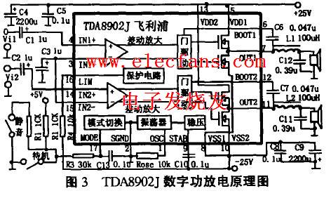
(3) Components with strong electromagnetic field radiation (such as L3, L2) and components sensitive to electromagnetic induction (R1, C1, R5, C3) should be shielded or kept away from electromagnetic field radiation sources to reduce interference.
(4) Shorten the connection between high-frequency components (such as R5, C3) as much as possible, try to reduce their distribution parameters and mutual electromagnetic interference. The susceptible components should not be too close to each other, and the input and output components should be as far away as possible.
(5) Some components or wires have a high potential difference, and the distance between them should be increased to avoid accidental short circuit during discharge. Such as ⑤, ⑦ of TDA8902J: ①, LH4652
â‘¢ The foot alignment should not be too close. Components with high voltage (such as power switches) should be placed in places that are not easily accessible by the hand when debugging.
1.2 Wiring principles
(1) The wires used at the input and output terminals (such as R8 and L1) should avoid adjacent parallels as much as possible. It is best to add a ground between the wires to avoid feedback coupling.
(2) The traces at all levels should be as short as possible, the components should be as close as possible, and more attention should be paid to large-signal and high-impedance traces. For example, the routing of R11 and C18 should be as short as possible, and the audio input (C1, R1) and output (L1, L2) lines should not be long, otherwise AC signals may be easily induced.
(3) The minimum width of the wire is mainly determined by the adhesion strength between the wire and the insulating substrate and the current value flowing through them. When the thickness of the copper foil is 0.05mm and the width is 1-15mm, the temperature through the current of 2A will not be higher than 3 ℃. The power amplifier can choose 0.5 ~ 5mm wire width. The minimum spacing of the wires is mainly determined by the insulation resistance and breakdown voltage between the wires in the worst case, which can make the spacing as small as 5 ~ 8mm.
(4) The rounded corners of printed conductors are generally rounded, and right angles or included angles will affect electrical performance in high-frequency circuits. Figures 1-2 (a) (b) (c) are the three types of corner lines. Figure (C) adopts 45 ° outer chamfered corner lines whose transmission performance and reflection performance are better than the other two corner lines. The performance of the rounded corner line is better than those of the three types of routing, but the scoring of the arc has higher requirements on the process of making the board, which will increase the production cost. Claim.
2.1 Power line design In the DC power supply circuit, changes in the load can cause power supply noise. According to the size of the PCB current, try to increase the width of the power line to reduce the loop resistance. This power amplifier circuit LM4651L part of the power supply wiring, the wire width is 1.5 mm to meet the requirements, and the LM4652 part requires 3 ~ 5mm. At the same time, the direction of the power line and the ground line and the direction of data transmission are consistent,
This helps to enhance noise immunity.
2.2 Ground wire design The ground wire is more important than the power cord. The main method to overcome electromagnetic interference is the design of the ground wire. The wiring of the ground wire is particularly particular, and the single-point grounding method is usually used. The analog ground, digital ground and high-power device are separated, and finally all are collected to the power ground. The power amplifier ground wire structure includes system ground, chassis ground, digital ground and analog ground. The design principles of the ground wire are:
(1) Separate the digital ground from the analog ground. The power amplifier has both a logic circuit and a linear circuit, they should be separated as much as possible, connected to the ground wire of the power supply end, and the ground area of ​​the linear circuit should be increased as much as possible. The ground of analog audio should use single-point parallel ground as much as possible.
(2) The ground wire should be as thick as possible. If the ground wire is very thin. The ground potential changes with the change of current, which makes the signal level of the power amplifier circuit unstable and the noise resistance performance deteriorates. Usually make the ground wire pass three times the current. The power amplifier grounding wire should be above 3 ~ 6mm.
(3) Correctly select single-point grounding and multi-point grounding. The analog part of the power amplifier has a low operating frequency, its wiring and the inductance between the devices have little effect, and the circulating current formed by the grounding circuit has a great influence on the interference, so single-point grounding should be used. When the working frequency of the digital part is greater than 10MHz, the impedance of the ground wire becomes very large. At this time, the impedance of the ground wire should be reduced as much as possible and the ground should be grounded at multiple points nearby. When the operating frequency is 1-10MHz, if a single point is used for grounding, the length of the ground wire should not exceed 1/20 of the wavelength, otherwise the multi-point grounding method should be used. Although the switching frequency of the digital part of the power amplifier is 125kHz, it is better to use multi-point grounding due to the influence of harmonics.
(4) Make the ground wire form a closed loop. The PCB of the digital power amplifier, the ground wire is designed as a closed loop can significantly improve the ability to resist noise. The reason is that there are many power-consuming components in the circuit. Due to the limitation of the thickness of the ground wire, a large potential difference will occur on the ground wire, resulting in a decline in the ability to resist noise. If the ground is formed into a loop, the potential difference will be reduced. , Improve the anti-noise ability of the power amplifier circuit.
2.3 Design of signal line When connecting with weak signals other than PCB, shielded cable is usually used. For high-frequency and digital signals, the shielded cable is grounded at both ends. The shielded cable used for the analog audio signal of the power amplifier is preferably grounded at one end. The signal traces in the PCB should be as short as possible and avoid interference sources. A simple electromagnetic interference model consists of three parts, as shown in Figure 3-1. This power amplifier contains a switching power supply, a high-power, high-current drive circuit, and a system containing a weak analog signal circuit and a high-precision A / D conversion circuit. Electromagnetic interference is inevitable. The purpose of EMC design is to make the power amplifier not only suppress all kinds of external interference, but also reduce its own electromagnetic interference to other electronic equipment.
3.1 EMC measures in PCB design The power amplifier pays attention to different layout areas, so that the width of the dedicated zero-volt line and the power line is ≥ 1mm, and the power and ground are distributed in a "well" shape. The current of the distribution line has reached a balance and is simulated The circuit specifically provides a zero volt line. In order to reduce crosstalk between lines, the distance between printed lines was increased, and several zero-volt lines were inserted as line-to-line isolation. PCB plugs are also arranged with two zero-volt lines as line-to-line isolation. Special attention was paid to the size of the wire loop in the current flow.
3.2 EMC of switching power supply supporting PCB
The power supply adds noise to the circuit while supplying power to the amplifier. The signal input, oscillation and control parts of the power amplifier circuit are most easily interfered by external noise. The strong interference on the electrical network enters the circuit through the power supply, and the analog signals in the circuit are most susceptible to interference from the power supply. The conduction disturbance and radiation disturbance of the power supply to the power grid are the non-linear flow and the common mode noise generated at the input end of the power supply by the coupling between the power transistor housing and the radiator in the primary circuit.
The power supply trimmed the switching voltage waveform, installed an insulating gasket with a shielding layer between the transistor and the heat sink, and added a mutual inductance filter to the mains input terminal, and reduced the loop area. A polyester film capacitor is connected in parallel with the soft recovery diode used in the stage rectifier circuit, so that the switching voltage waveform has been greatly improved.
3.3 EMC of the transmission line
Coaxial cable has better resistance to electromagnetic interference. The coaxial cable used for this power amplifier signal line is the American AUDIOOUEST (line Saint), using single-ended grounding, which reduces the loop current for magnetic induction and enhances the magnetic field shielding performance. 
