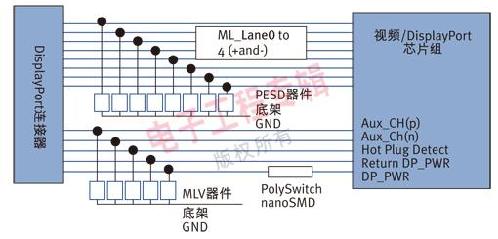
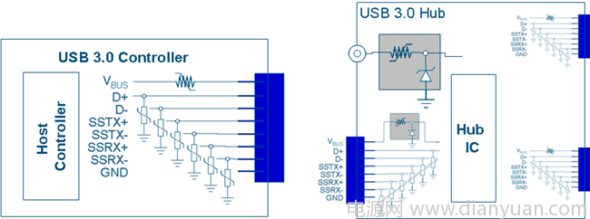
Design of high-frequency data transmission interface circuit protection scheme The continuous development of IC process technology and the popularity of high-speed data transmission interfaces make related ESD protection increasingly difficult. The strong demand for faster processing speed and higher functional density has pushed IC manufacturers to further reduce the minimum size of MOS components, especially when the manufacturing technology shifts to below 90nm, IC chips are getting smaller and smaller, higher and higher density, and more functions. It is becoming more and more complex, and the electromagnetic environment it uses is becoming increasingly harsh, which makes it more susceptible to damage from ESD, overvoltage and overcurrent. At the same time, the continuous development of various high-speed interfaces, especially the rapid growth of portable multimedia devices, makes high-speed data transmission inevitable. How to ensure the high-speed transmission of data while protecting the interface security has become a problem faced by high-frequency data interfaces. Circuit protection requirements for different interfaces Among the current mainstream interfaces, USB is the most widely used, and the latest USB3.0 will support transmission speeds up to 5Gbps. When the transmission speed is increased to such a high level, the signal retention time is only 200ps. At this time, traditional high-capacitance MLV, TVS and other devices will not be used for ESD protection. High parasitic capacitance will seriously cause signal waveform distortion: it reduces the level The hold time makes the rising and falling edges of the signal change so much that the signal cannot reach the normal working level. In contrast, the HDMI 1.3 standard doubled the data transfer rate of the early HDMI 1.0-1.2 to 3.4 Gbps per pair of differential signals. To achieve such a high data transfer rate, low capacitance and excellent circuit board design will become the key to fully ensure signal integrity. The new DisplayPort interface is also being adopted by many personal computers, monitors, projectors, and other display content (playback) source designs. The DisplayPort interface operates at a rate of up to 2.7Gbps, which is much higher than the original video / multimedia interconnection standard, and therefore faces the same challenges. Hard disk drive, computer and set-top box manufacturers are aligning with the E-SATA (External Serial ATA) standard as a fast way to transfer video between storage devices. The latest transmission bandwidth defined by the latest SATA3.0 standard will be as high as 6Gbps. E-SATA technology's requirements for ESD are very similar to HDMI and DisplayPort. The hot-swappable nature of E-SATA makes high-level ESD protection particularly critical. It can be seen that for designers, the complexity and difficulty of high-speed interface circuit protection design comes from the working speed, and many designers feel incapable of starting with a variety of speed expressions. Taking HDMI1.3 and DisplayPort as examples, HDMI1.3 generally refers to working at a data transmission speed of up to 10Gbps at 340Mpixel / s. The highest transmission speed here means that the interface will be based on the video capabilities of the connected generator and receiver. Change its clock rate. The higher the resolution or color depth of the two connected devices, the higher the clock frequency. For example, high-definition video has more data to process in 1,080p mode than in 1,080i mode, and the clock rate is faster. In actual work, the working speed of HDMI depends on the capabilities of the transmitter and receiver and the resolution and color depth of the playback source. Figure 1 shows the maximum operating speed of TMDS for commonly used high-speed interfaces. The DisplayPort standard specifies two operating speeds: 1.62GHz and 2.7GHz. Designers can choose a lower working speed according to specific uses and cost factors, and a higher speed can make the refresh speed faster, higher resolution, and richer color depth. In some cases, it is also possible to implement designs with two speeds. The latest USB 3.0 specification greatly increases the demand for low capacitance ESD devices. USB 3.0 adds two high-speed differential signal pairs to the existing USB 2.0. Due to the ability to transmit and receive differential signal pairs up to 5GHz, USB 3.0 requires signals to be 50% faster than DisplayPort. At this speed, any additional capacitors will affect the eye diagram and thus compliance with the USB 3.0 specification. The main difficulty of the above high-speed data transmission interface circuit protection is that the excessive parasitic capacitance of the protection device will cause a certain degree of signal attenuation, thereby reducing the display quality. Therefore, ESD devices should choose ESD devices with sufficiently low capacitance and stable ESD shunt capability according to the signal frequency of the circuit interface they protect, and choose between component size, ESD protection performance, and convenience of implementation. When adding ESD protection to the high-speed data interface circuit, the timing effect of the added capacitor and inductor on the high-speed differential signal must be considered. When USB3.0 works at speeds up to 5GHz, any additional impedance on the line may distort the signal, making it difficult to meet the signal rise time specified in the eye diagram and maintain the signal level. Choose the right ESD protection device The timing performance of high-speed signals is generally measured with an eye diagram, which is an analysis tool used to accurately display timing and comment errors. As shown in Figure 2, the gray part in the middle of the eye diagram represents the electrical specifications of the high-speed differential signal. When the line gradually invades the gray part, the error margin becomes smaller and smaller. The eye width is an ideal indicator that represents the data line stabilization time and whether there are errors. Eye height indicates the signal level or amplitude. Since TMDS pairs are differential signals, it is important to minimize the differential capacitance and signal-to-ground capacitance to ensure that the rise and fall times of the signal meet the requirements. The ideal situation is that the capacitance is low enough to give the designer enough design margin. In order to meet the requirements of high-speed data communication interface, it not only makes ESD protection effective, but also does not affect the high-speed signal transmission. In recent years, a variety of devices specifically adapted to such protection requirements have been launched on the market, such as the polymer ESD suppression device PESD and the low-capacitance silicon ESD device SESD introduced by Tyco Electronics Raychem Circuit Protection. The capacitance of PESD devices is extremely low, with a typical value of 0.25pF, and the leakage current is extremely small (<0.001A); ESD protection is fast and effective, and the price is lower than that of low capacitance silicon devices. The low-capacitance silicon ESD device introduced by Tyco Electronics includes 0201 package, SESD0201C-006-058 with a typical capacitance of 0.6pF, 0402 package, and SESD0402S-005-054 with a typical capacitance of 0.5pF. Figure 2 shows the eye diagram performance of Tyco Electronics 0.25pF PESD device operating at 3.4GHz (HDMI 1.3). As shown in the figure, when the interface transmission speed is up to 3.4GHz defined by HDMI1.3, Tyco Electronics PESD is used. During the transmission of the signal of the electrostatic protection element, there is sufficient margin in the signal rise time, fall time and signal level to ensure that the normal data transmission is not affected. Low insertion loss and stable capacitance covering a wide frequency range also have an important impact on achieving the ultimate goal of adequate protection, cost savings, and minimum signal attenuation. Insertion loss is an important indicator of signal attenuation-frequency relationship. Insertion loss is too high will reduce the device and system bandwidth, and bring additional design constraints to meet the eye diagram level. The capacitance and frequency characteristics of ESD protection devices may also affect the design performance of high-speed ports, thereby increasing design constraints. In high-speed systems, circuits designed for a particular capacitor may behave differently due to different ESD protection methods used, which forces designers to use complex software process improvements and capability determination (SPICE) when conceiving HDMI circuit protection mechanisms. ) Model and simulation means. Figure 3 and Figure 4 show the insertion loss of Tyco Electronics' two SD devices for high-speed data transmission interface protection E at high-frequency transmission rates. Compared with other polymer ESD protection devices, Tyco Electronics' PESD has lower trigger voltage and clamping voltage, withstands ESD shocks, and has a long life; SESD has a slightly higher capacitance (0.6pF) than polymer PESD components. , But its trigger voltage and clamping voltage are relatively lower, which has better protection for extremely sensitive ICs. The two products launched by Tyco Electronics can completely cover the protection of high-speed data transmission interfaces. Designers can choose according to the protection level, operating frequency of the interface circuit, component size, cost, and convenience of implementation. These two series of products adopt the most popular 0603, 0402 and the smallest 0201 package in the electronics industry. They meet the strict RoHS requirements and can help set-top box sensitive circuits, laptops, mobile phones and other portable devices from ESD. PPTC overcurrent protection For security and adjustment considerations, the HDMI, USB, and DisplayPort specifications also require end-user-accessible power connectors to implement overcurrent protection. The overcurrent protection device must be able to reset without mechanical intervention by the user. To prevent misoperation, the preset operating limit must be higher than the allowed transient current. At the same time, the normal resistance of the protection element must be low enough to avoid too much voltage drop. The effect of polymerized positive temperature coefficient (PPTC) devices in various high-speed interface applications has been proven. As with traditional fuses, they will limit the loop current when the current exceeds the specified limit current. However, unlike the fuse, PPTC can be reset after the fault is cleared and the power is turned on again. PPTC devices have the characteristics of low resistance, fast action time and small size, making them the preferred method for overcurrent protection in many power supply bus architectures. Unlike HDMI and DisplayPort, the USB interface is usually used to provide functions such as power supply and charging for portable electronic products. Therefore, downstream devices that are powered or charged by the USB interface will be harmed by inductive voltage spikes, wrong chargers, and reverse bias. Tyco Electronics' polyZen element is a polymer-protected precision Zener diode micro-integrated module, which is composed of a stable clamping voltage accurate Zener diode and a nonlinear polymer PTC (positive temperature coefficient). The transition from a low-resistance state to a high-resistance state in response to diode overheating or overcurrent faults. PolyZen components are resettable to prevent high-power fault events, while only consuming 0.7W. When the diode overheats or overcurrent occurs, the PTC "acts" to limit the current and generate a voltage drop, which helps protect the Zener diode and the electronic equipment behind it, thereby effectively improving the power handling capability of the diode. Figure 5, Figure 6 and Figure 7 show the HDMI1.3, USB3.0 and Display port interface protection circuit schematics designed with Tyco Electronics ESD devices, MLV devices, PolySwitch overcurrent protection devices, and PolyZen overcurrent and overvoltage protection devices. Figure 5 Typical HDMI interface circuit protection scheme design-ESD and overcurrent protection Figure 6 Typical DisplayPort interface circuit protection scheme design-ESD and overcurrent protection Figure 7 Typical USB3.0 circuit protection scheme design-ESD, overcurrent and overvoltage protection Grinder Machine,Surface Grinding Machine,Grinding Equipment,Tool Grinding Machine Hunan Furui Mechanical and Electrical Equipment Manufacturing Co., Ltd. , https://www.thresher.nl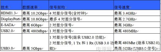
Figure 1. Comparison of signal speed requirements for different high-speed interfaces 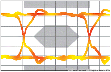
Figure 2 Eye diagram of Tyco Electronics' 0.25pF PESD device operating at 3.4GHz 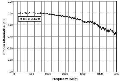
Figure 3 Tyco Electronics Raychem PESD device insertion loss curve 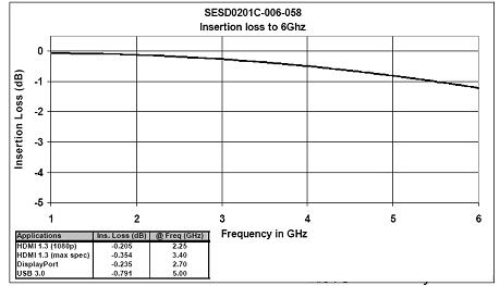
Figure 4 Tyco Electronics Raychem SESD device insertion loss curve