ã€Abstract】The hardware structure of TMS320DM642 digital signal processor is briefly introduced. The general flow of program optimization for DSP platform is given briefly. The TMS320DM642 platform optimized X264 video encoder is studied, including algorithm and system structure optimization, ping-pong buffer optimization, loop body optimization and DSP assembly implementation. This article refers to the address: http:// Oilfield Gas Generator,Gas Power Generator,Green Power Gas Generator,Small Gas Generator Jiangsu Vantek Power Machinery Co., Ltd , https://www.vantekpower.com
1 Introduction
In the digital video application scheme, the video encoder is the core, in which the hardware computing capability of the encoder is the guarantee of the real-time performance of the system, and the high compression ratio of the video compression standard provides the necessary guarantee for the encoder to adapt to various transmission bandwidth channels. Video coding project X264 is an open source video encoder developed on the PC platform according to the H.264 standard. If you directly migrate to the TMS320DM642 (hereinafter referred to as DM642) platform, the actual encoding speed is generally lower than that required by the video application solution. Real-time requirements. In order to improve the coding speed of the coding project, it is necessary to optimize the X264 transplanted to the DM642 platform. The entire optimization process is shown in Figure 1. 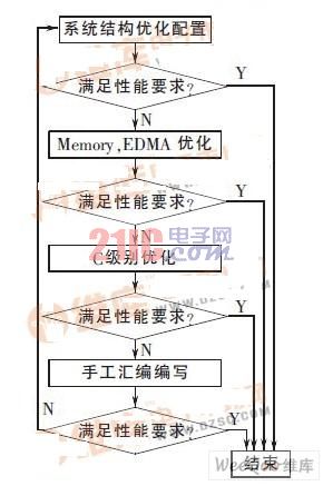
Figure 1 Optimization flow chart
2 DM642 hardware introduction
The DM642 uses the VLIW architecture of the second generation of high-performance advanced VelociTI technology developed by TI to achieve a processing speed of 4 800 MI/s (mega-instructions per second) at a frequency of 600 MHz. The DM642 CPU core has 64 32-bit general-purpose registers and 8 independent 32-bit arithmetic units (2 multipliers and 6 arithmetic logic units), ensuring four 16-bit media access controls per cycle (Medium Access Control) , MAC).
The DM642 uses two levels of cache, L1 and L2. The first level cache L1 includes a first level program cache L1P and a first level data cache L1D; the second level cache L2 can be configured as on-chip memory, a cache, or a combination of the two.
Peripherals include [4-6]: 3 configurable video ports; 1 10/100 Mbit/s Ethernet controller (EMAC); 1 management data input and output (MDIO); 1 interpolated VCXO control Interface; 1 McASP0; 1 I2C bus; 2 McBSPs; 3 32-bit general-purpose timers; 1 user-configured 16-bit or 32-bit host interface (HPI16/HPI32); 1 PCI; 1 16-pin General-purpose input and output (GP0) with programmable interrupt/event generation mode; a 64-bit IMI-FA that can be connected to peripherals of synchronous and asynchronous memories.
Like the traditional DSP, the DM642 adopts the Harvard architecture, which separates the data from the program in different storage areas, ensuring that the instruction from the program memory area and the operation data from the data memory area are independent of each other in the actual operation of the DSP. In addition, 8 different processing units are designed inside the CPU, so that the CPU can operate according to the pipeline process during the running process.
3 DM642 platform optimization program introduction
3.1 Optimization of algorithm and system program structure
The system structure optimization is mainly to reasonably arrange the position of each module in the storage interval of the DSP, that is, to solve the mapping problem of the storage interval; in the aspect of data processing, minimize the unnecessary movement of the data to be processed. Algorithm optimization is mainly reflected in whether the analysis algorithm has a better and simpler alternative method, whether the algorithm has some symmetry, whether it can adopt a more appropriate data structure. In the optimization of X264, first consider the reasonable arrangement of the system structure, such as program to memory mapping, firstly use the CCS CODE_SECTION[9] pseudo-instruction to map the 9 large modules in X264 to 9 large sub-intervals. Inside, the frequently used DCT/IDCT module, QUANT/DEQUANT module, SAD/SATD module are placed in the DM642's on-chip memory area (L2 SRAM), and other modules are mapped to the off-chip memory area. In terms of data access, it is considered that the X264 code allocates storage space for the reference frame in the encoding frame and the inter prediction, respectively. In the process of migration, there are problems in the storage location of the encoded frame and the reference frame. From the perspective of access speed, the access speed of the on-chip storage area is much higher than that of the off-chip storage area, but the space of the on-chip storage area is much smaller than that of the off-chip storage area, which results in access speed and limited space. Contradictions between. Considering the actual coding process, the basic unit of coding is a 16×16 luma macroblock plus two 8×8 chroma modules, where the CCS DATA_SECTION[9] pseudo instruction is used in the on-chip memory area of ​​the DM642 (L2SRAM). Apply for 2 storage areas of size (16×16+8×8+8×8) to store the encoded pixel values; use the DATA_SECTION directive to apply for some space in the on-chip storage area, and temporarily store the encoding during encoding. Intra prediction mode information, inter prediction motion vector information, and discrete cosine transform coefficients and quantized coefficients of a macroblock; finally, a reference memory block is allocated a certain storage space for motion estimation and intra prediction reference. The entire current coded frame and motion estimation reference frame are placed in the off-chip memory area of ​​the DM642 map.
3.2 Optimization of EDMA and Ping Pong Cache
EDMA (Enhanced Direct Memory Access) is an abbreviation for Enhanced Direct Memory Access. DMA technology refers to data migration between peripherals and peripherals, between peripherals and memory, and between memory and memory without CPU intervention on embedded processing platforms or large computing platforms. access. This ensures that when the CPU is operating on a set of data, the memory prepares the new experimental data to be processed, reducing CPU latency, especially in cases where large amounts of data need to be moved, which can significantly improve the system. calculating speed. The DM642 has 64 EDMA physical transport channels to ensure that data is moved between the DM642 peripheral's buffer interval and the DM642 memory in a very short time. The DM642's EDMA[10] has three main startup modes: CPU startup, synchronization event startup, and external event startup.
CPU startup refers to the CPU launching a pre-configured EDMA migration task by calling the EDMA Application Programming Interface (API). Synchronization event initiation generally refers to an EDMA channel completing the migration task and generating an excitation signal to trigger other EDMA channels to begin data movement. External event initiation generally refers to the DSP's peripherals completing the data exchange with the outside world, and then exciting the EDMA channel for data movement.
In the EDMA optimization of X264, the dual buffer mechanism, also known as the ping-pong buffer mechanism, is adopted. The specific operation code example is: 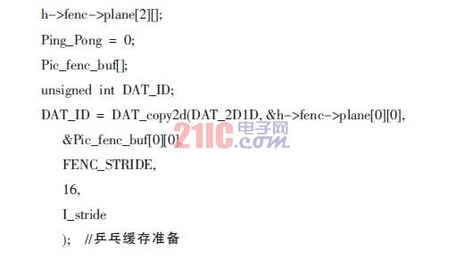
In the example, the variables Ping_Pong and DAT_ID are defined in addition to the data storage source and destination addresses required for data movement. Ping_Pong is a flag variable that indicates whether the destination storage area for storing the moved data is the Ping storage area or the Pong storage area. DAT_ID is the handle variable of the ongoing EDMA move. Before entering the official encoding loop body, EDMA will move a macroblock pixel value to be encoded to the Ping memory area in advance (assuming Ping_Pong=0 means Ping memory area). After entering the loop body, first alternate the target storage area (Ping_Pong=1-Ping_Pong, then Ping_Pong=1, indicating Pong storage area), and then wait for the previous move to complete (DAT_wait(DAT_ID)), if the previous move is completed , you can immediately start the next move, and the CPU immediately processes the move data. Subsequent operations are similar until all macroblocks have been encoded, ending the loop body.
3.3 Optimization of the loop body
In the X264 video encoder, the loop body appears at a higher frequency, and often the loop body is the more time-consuming part of the entire encoder. Especially when loop body nesting occurs, or there are logic judgment statements or function calls inside the loop body, the compiler generally does not optimize the loop. For these problems, the more common methods are nested loop body inner loop expansion, using conditional operators instead of logic judgment statements, using inline functions, using the MUST_ITERATE directive operator [11-12], splitting the large loop body into several A small loop body. The example code for the loop body optimization I use is: 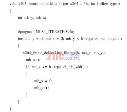
In the above example, the directive MUST_ITERATE mainly tells the encoder that this loop will execute a total of 396 times, so that the compiler can perform software pipeline to optimize the loop.
3.4 compiler optimization options
After completing the above manual optimization, the next step is to use compiler optimizations by setting compiler options. The compiler optimization options used in this article are: -pm (optimized at the program level), -o3 (the strongest at the file level) Optimization), -op3 (the most important speed), -ml3 (by default all data and functions are type far).
3.5 DSP assembly optimization
If you use the above optimization strategy to optimize the coding project, the speed of the encoder can not meet the application requirements, you need to write a manual assembler. Before writing a manual assembler, first use the CCS profile tool to parse the coding project, find out the parts of the function that are time-consuming or frequently called, and rewrite these parts into assembly functions.
The DSP uses a Harvard architecture that separates data and programs. In general, the main steps in writing assembly language functions are: taking the operands out of memory and putting them into the registers of the CPU, and then operating the operands in the registers with different arithmetic units inside the CPU, and finally the result of the operation. Save to memory. Among them, the function parameter transfer, function return value register, condition register, stack pointer register must be saved in accordance with the provisions of the corresponding register, otherwise an error will occur.
The following aspects should be considered in the process of writing assembly language: 1) Fully understand the logical functions of the function to be written. Only by truly understanding the functions of the function implementation and the specific data flow diagram can the assembly language architecture be more efficient; 2) the selection and arrangement of the data structure. Since DM642 allows data packing processing, that is, an instruction can operate on several bytes at the same time, which is very beneficial for image and video processing, so package processing can be packaged as much as possible; 3) Register allocation and instruction sequence . The DM642's CPU has 2 sets of fully symmetrical arithmetic units and registers. As long as the operands are stored separately and taken into the registers belonging to different sets, different arithmetic units are used, and the order of the instructions is arranged reasonably to ensure that more instructions are arranged in one cycle under the condition that resources do not conflict. The efficiency and parallelism of instruction execution.
Let's take an example of SAD_4×4 to illustrate how the above items are implemented. The code for the C language version of SAD_4×4 is: 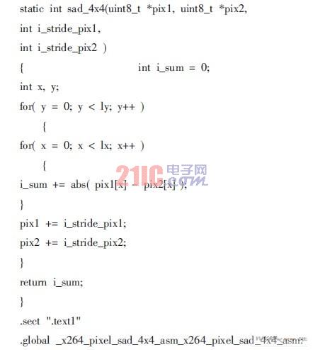
The code for the assembly language version of SAD_4×4 is: 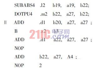
After the assembly instructions are written, the assembly language is debugged. Since the X264 project is relatively large, if it is difficult to debug directly in the project, a small project is created during the debugging process, and a piece of data is read from the file to test the correctness of the assembly language function. The specific steps are: while using single-step debugging, turn on the view memory and view core registers options in the debugger CCS to see if the values ​​in the corresponding memory and registers are changed according to the logic design. If the result is incorrect, consider whether the register is used incorrectly, or if you have not waited for enough delay cycles, or if the order of the instructions is incorrectly arranged for the purpose of software pipeline until the error is found.
4 Summary
The author first analyzes the X264 encoding project after porting from the PC platform to the DSP platform. The encoding rate is low, which can not meet the real-time requirements of video compression. Then, from the perspective of improving the encoding speed of the encoder, the coding engineering is optimized. Several DSP platform optimization methods used in practice are introduced: optimization of algorithm and program system structure, EDMA and ping-pong cache optimization, loop body Optimization, compiler optimization, and DSP assembly. The CIF format image is encoded by BASE_LINE. The optimized X264 encoding speed is about 5~8 f/s (frame/second), and the optimized encoding speed is about 20 f/s. The speed is obviously improved, and the real-time encoding can be realized. .