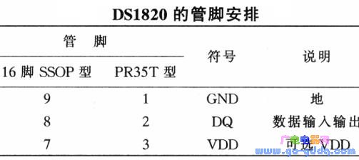
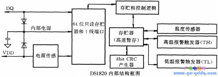
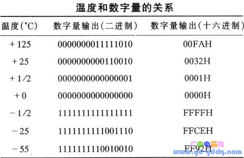
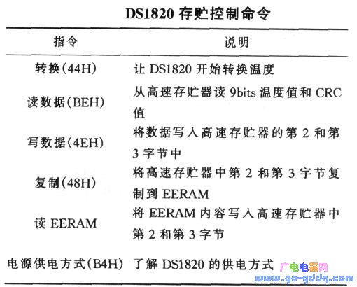
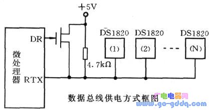
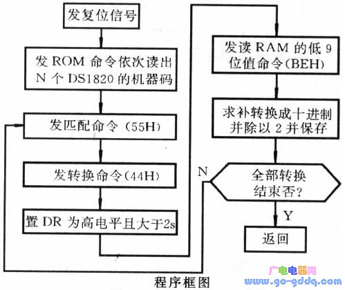
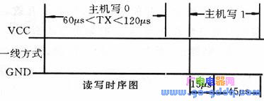
The DS1820 is a one-line digital thermometer developed by Dallas that uses a 9-bit digital representation of temperature. It allows multiple DS1820 strings to be on a single data line, minimizing the number of I/Os connected to the microprocessor. The function and working mode of integrated circuit chip DS1820 are introduced in the paper, and application examples are given. 1. The main features of the DS1820 The DS1820 has the following main features: (1) Communication can be completed with only one I/O line; (2) Multiple dispersed DS1820s can share the same line for communication; (3) No external components are required; (4) can be powered by the data line; (5) The detection temperature range is -55 to +125 °C, and the accuracy is 0.5 degrees; (6) The temperature is represented by a 9-bit digital quantity; (7) It takes 200ms to convert the temperature into a digital quantity each time; (8) A temperature that does not change can be defined as the alarm temperature; (9) Available in PR35T and SSOP packages. 2.DS1820 pin arrangement The pin assignments for the DS1820 are listed in the table below. 3DS1820 internal structure and workpiece process 3.1DS1820 internal structure The internal block diagram of the DS1820 is shown below. As can be seen from Figure 1, the DS1820 consists of the following components: (1) 64-bit laser read only memory. The unique serial number of each DS1820 is stored here. The first 8 digits are the product type number (DS1820 is 10H), followed by the unique serial number of each device. There are 48 digits, and the last 8 digits are the first 56 CRC schools. Code verification. This is why multiple DS1820s can communicate in one line. (2) Temperature sensor. It is a key part of turning temperature into digital. (3) Memory of the DS1820. It consists of a high-speed memory RAM and EERAM (high-temperature TH and low-temperature TL alarm flip-flops). The data is first written to the high-speed memory RAM and then written to the EERAM by a copy command. The high-speed memory RAM consists of 8 bytes. The first two bytes store the value of the detected temperature, the 0th (LSB) is the value of the storage temperature, and the 1st (MSB) stores the sign of the temperature value. If the temperature is negative, Then the first memory is all 1, otherwise it is all 0, which is why 9bit can be used to indicate the temperature. The lowest bit is read first. If the lowest bit of the LSB is 1, it is expressed as 0.5 degree. The method of evaluation is based on the value in the MSB, and the binary number in the LSB is complemented and converted into a decimal number divided by 2 to obtain the value of the measured temperature. The above table is the relationship between temperature and digital quantity. The second and third bytes are values ​​copied from TH and TL, when power-on is updated; the next two bytes are useless, if read it should be all l; the sixth and seventh bytes are count registers The last byte is the CRC check. (4) Optional power supply VDD. Each DS1820 can be set to two power supply modes, namely data bus power supply mode and external power supply mode. The external power supply mode is the same as the general circuit. Data bus power supply is parasitic power supply, which also provides conditions for multiple DS1820 strings together. This parasitic power supply supplies power whenever I/O is high. Since the DS1820 requires 1mA of current during conversion, the conversion time needs to be longer. The block diagram is shown in Figure 2. 3.2 Working process The microprocessor communicates with the DS1820 through an I/O line. The microprocessor first sends a reset pulse, and then receives a reset pulse. At this time, the ROM command is issued, and the memory and control commands are sent (the ROM is not sent to the DS1820). Sending and controlling commands before the command does not work). 3.2.1 DS1820 ROM Command The DS1820 ROM commands are as follows: (1) Read ROM (33H), which is the serial number of the read 1820; (2) Match ROM (55H), which is a command to read the 64-bit serial number for the purpose of positioning multiple DS1820s; (3) Positioning ROM (CCH), which can be used in the case of only a single DS1820 The first command; (4) search ROM (FOH), it is for when the system does not know is Which DS1820 is online; (5) Alarm search (ECH), which is used to search for which device alarm. 3.2.2 DS1820 storage control commands The DS1820 storage control commands are listed in the table below. 3.2.3 DS1820 execution sequence (1) Initialization (sending a low pulse of not less than 480 μs); (2) Execution of the ROM command, mainly for positioning; (3) Execution of the DS1820 storage control command for converting and reading data; (4) DS1820 The I/O signals include reset pulse, response pulse, write 0, read O, write 1 and read 1. Except for the response pulse sent by the DS1820, the rest is sent by the host. 4 applications When we were making the measurement and control system of the program-controlled computer room, because there were many equipments in the equipment room and many points to be tested, the DS1820 was selected to detect the temperature, so that multiple DS1820s could be strung on one line, saving the power module. The circuit is shown in the figure above. The block diagram is shown below. All the programs are debugged and run for a long time, and the performance is good, which can meet the needs of users. In actual use, we also found the following notable problems: (1) The reset signal time of the DS1820 cannot be short, preferably 1ms, otherwise the subsequent commands may not be executed. (2) Although the serial number of each DS1820 is unique, it is not possible to string multiple DS1820s together to read the serial number. It must be read out one by one before being stringed together. (3) Due to the bus power supply mode, the operating current of the DS1820 during temperature conversion is greater than 1 mA. Therefore, the DR in Figure 2 must be set to 1 during the conversion to make the FET turn on, so that the data bus is directly connected to the +5V power supply. Interconnected and maintained for more than 2s, to ensure the time required for the temperature conversion of the DS1820, because the power supply through the 4. 7kΩ pull-up resistor is insufficient to provide the current required for DS1820 conversion. (4) It is not possible to communicate with the DS1820 using the communication method of the serial port of the single-chip microcomputer, but it can be used as an I/O port. (5) Due to the write time slot relationship of the DS1820 (see the figure below), writing 1 after writing 0 must have a low pulse of 800 μs, and writing 1 after writing 1 is also true, otherwise the read data will be wrong. A membrane switch consists of various layers laminated together. The layers of a basic membrane switch construction include: a membrane overlay, spacer, printer circuit, rear adhesive, and tail filler. Depending on the environment and requirements of the application into which the membrane switch plugs into, the construction can vary. Membrane Switch Assemblies,Lcd Display Membrane Switch,Tactile Membrane Switch Keypad,Overlay Tactile Membrane Switch KEDA MEMBRANE TECHNOLOGY CO., LTD , https://www.kedamembrane.com