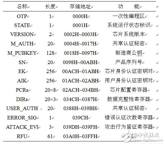
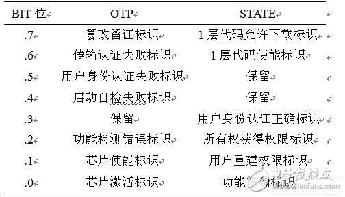
introduction In order to meet the needs of smart cards and trusted computing applications, a dedicated SoC chip was designed and implemented. The chip consists of a microprocessor, program and data memory and management module, security logic module, cryptographic service module, auxiliary function module, I/O interface, which can provide confidentiality, integrity and identity authentication for various security applications. A cryptographic service, as well as applications such as data storage, access control, and secure computing. The design of the security control architecture of the dedicated SoC chip should first analyze the application environment of the chip, and obtain the threat model and deployment model of the chip, namely the potential attacker and possible attack mode of the chip, as well as the production, transportation, development and use of the chip. The risk problem of the link; secondly, according to the chip security requirements and functional specifications, through the software and hardware collaborative design, set the relevant hardware logic, status register and parameter storage area, and implement the software control process of the relevant security policy; The system performs safety analysis, simulation verification and FPGA testing. 1 chip system security architecture design Based on the actual production and application of the chip system, according to the importance of the protected assets on the security of the chip and the information technology security evaluation criteria, the protected assets of the chip can be designed as the following three security levels. Level 0 assets: integrity and credibility of the O layer code, confidentiality, integrity and credibility of the layer 0 data (LEVEL0), and the correct function of each module of the chip. Level 0 assets are the security foundation of the chip system, and failure to protect any of them will result in the entire chip system refusing to provide any services. Level 1 assets: integrity and credibility of layer 1 code, confidentiality, integrity and credibility of layer 1 data (LEVEL1). Level 1 assets are the core control state of the system operation and the security foundation of the level 2 assets. Failure to protect the level 1 assets will prohibit the execution of this layer code and layer 2 code. Level 2 assets: Layer 2 code integrity and credibility, confidentiality, integrity and credibility of Layer 2 data (LEVEL2). Level 2 assets are the top-level protected assets of the chip system. Failure to protect the assets of this level will result in the code being disabled. Level 2 assets can exist in the chip system at the same time, but only one is put into operation at a time. 1.1 chip system security state design After the chip is powered on, it can obtain different security rights by executing a series of commands, and thus is in a certain security state. ST1: Factory default state. Under the premise of trusting the manufacturer, the chip can be trusted at the factory initial state. The initial state is the trusted basis of the chip. ST2: Chip enable status. When the power is first applied, the status of the chip is after the power-on self-test and transmission security certification. The chip is verifying that each functional module is correct and that. After the layer code and data integrity check are passed, the transmission process security authentication command is received, and the shared secret of the developer and the manufacturer is utilized, and the chip is authenticated within the allowed number of authentication times. ST3: Chip activation status. The chip is enabled, allowing the developer to complete user creation through user-created commands. In this process, the legality of the chip's identity to the developer depends on the shared secret when transmitting the security certificate. After the user is created, the chip activation status indicator and ownership are identified. When launched again, the identity legality of the developer depends on the shared secret entered and the user key created by the developer. ST4: Layer 1 code download permission status. To meet the flexibility of chip usage, the chip's Layer 1 code can be configured by the developer. The code download needs to authenticate the initiator of the download command. Within the range of allowed authentication times, if the identity authentication is correct, the layer 1 code download permission flag is set, and the chip enters the layer 1 code (chip operating system) download permission state. ST5: Layer 1 code download completion status. Complete the layer 1 code download under the control of the download control program. After the download is completed, the download control program calls the SHA1 module to perform integrity measurement and storage on the layer 1 code and compare it with the input download code integrity information. If the integrity verification is correct, the layer 1 code enable flag is set. ST6: Layer 1 code running status. The chip system can be transferred from ST3 and ST5 to the 1-layer code running state. Before entering this state, it is necessary to judge whether the layer 1 code enable flag is valid, and enter the code running state after verifying the layer 1 code and data integrity is correct, and execute the corresponding program to complete the predetermined function. ST7: Layer 2 code (user application) download permission status. The download and invocation of the 2-layer code are completed under the supervision of the layer 1 code. In the layer 1 code running state, if the user inputs a layer 2 code download command, the layer 1 code first authenticates the code download command initiator identity. Within the allowed number of authentication times, if the identity authentication is correct, the layer 2 code download permission flag in the sensitive information memory of the layer is set, and the chip enters the layer 2 code download permission state. ST8: The 2-layer code download completion status. As with the download process of the 1-layer code, the download of the 2-layer code is completed by calling the download control program. After the download is completed, the layer 1 code performs integrity measurement and storage on the layer 2 code, and compares the integrity information of the input. If the integrity verification is correct, set the Layer 2 code enable flag in LEVEL1. ST9: Layer 2 code running status. When the 2-layer code and data integrity verification is correct, the chip system can be transferred to the Layer 2 code running state by ST6 and ST8. When the 2-layer code enable flag is valid, the chip system can enter the layer 2 code running state through the hierarchical jump instruction under ST6 or ST8. In the ST6 state, the chip system can also complete its corresponding operation and control functions by calling 2 layers of code. Different from the hierarchical jump into ST9, when the corresponding function is completed by calling the 2-layer code, the chip system can return to ST6 after the execution of the 2-layer code. When entering the ST9 through the hierarchical jump command, the chip system remains at ST9 after completing the specified function, or returns to ST3 through system reset, and does not allow it to return to ST6. 1.2 Status Bits and Control Parameter Settings In order to achieve the normal jump between the above states, the chip system needs to set corresponding status bits and control parameters to register the control information and working state of the chip during operation. The status bit and control parameter setting are the basis for the establishment of the chip security architecture. Based on the division of the privilege state of the chip, refer to the configuration of the status bits and control parameters of the TPM and ATMELSC series security chips, and use LEVEL0 as the status bit and control parameters of the dedicated SoC chip. Storage area, its specific settings are listed in Table 1. Table 1 LEVEL0 status bit and control parameter configuration table In Table 1, the OTP (One TIme Programmer) area is a one-time programming area for the permission identification and status retention of the chip once. STATE is the system status identifier, which is used to identify the current permission status information of the chip. The correspondence between the roles and bits of each bit in OTP and STATE is shown in Table 2. Each of them is active high. Table 2 Status Bit Function Table in OTP and STATE M_AUTH is the shared secret between the manufacturer and the developer, M_PUBKEY is the manufacturer's public key, and SN is the product serial number, which are used together for the chip's transmission process security certification. EK (Endors- ement Key) is the identity authentication key pair of the chip system. In the actual application process, the chip signs the data by calling the EK private key to indicate its legal identity. AIK (Attes-taTIon IdenTIty Key) is a developer identity key pair. It is generated by the on-chip random number and the RSA algorithm IP core during user identity creation for user identity authentication. PCR (Pla-tform. ConfiguraTIon Register) is the platform configuration integrity registration area. In order to meet the hardware scale limitation of the chip system during the FPGA test of the dedicated SoC chip, eight PCRs are temporarily configured for the chip system, and each PCR register is 20 bytes. Except for PCR6 and PCR7, the expressions of the remaining PCR registers are as follows. PCR0 = SHA1 (DOWNLOAD) PCR1 = SHA1(LEVEL0) PCR2 = SHA1(COS) PCR3 = SHA1(APPLI) PCR4 = SHA1(LEVEL1) PCR5 = SHA1(LEVEL2) DIR (Data Integrity Register) is the data integrity register of the chip system, which registers the internal data and code integrity information of the chip. In the specific design, three DIRs are configured for the chip system to store three levels of data and code integrity. Sex, the expression of the information stored in each DIR register is as follows. DIR0 = SHA1(PCR0||PCR1) DIR1 = SHA1(DIR1||PCR2||PCR4) DIR2 = SHA1(DIR1||DIR2||PCR3||PCR5) USER_AUTH is the shared authentication secret of the user and the chip system. When the user is created, the user's identity verification is completed through the corresponding command input. ERROR_SIG is the authentication error count register, which is used by the chip system to protect against dictionary attacks. ATTACK_EVI is the attack retention register, which registers the number and manner of physical attacks on the chip system. Led Surface Panel Light,Direct-Lit Led Panel Lamp,Direct-Lit Led Panel Light,Surface Mounted Panel Light Changxing Fanya Lighting Co.,Ltd , https://www.fyledlights.com